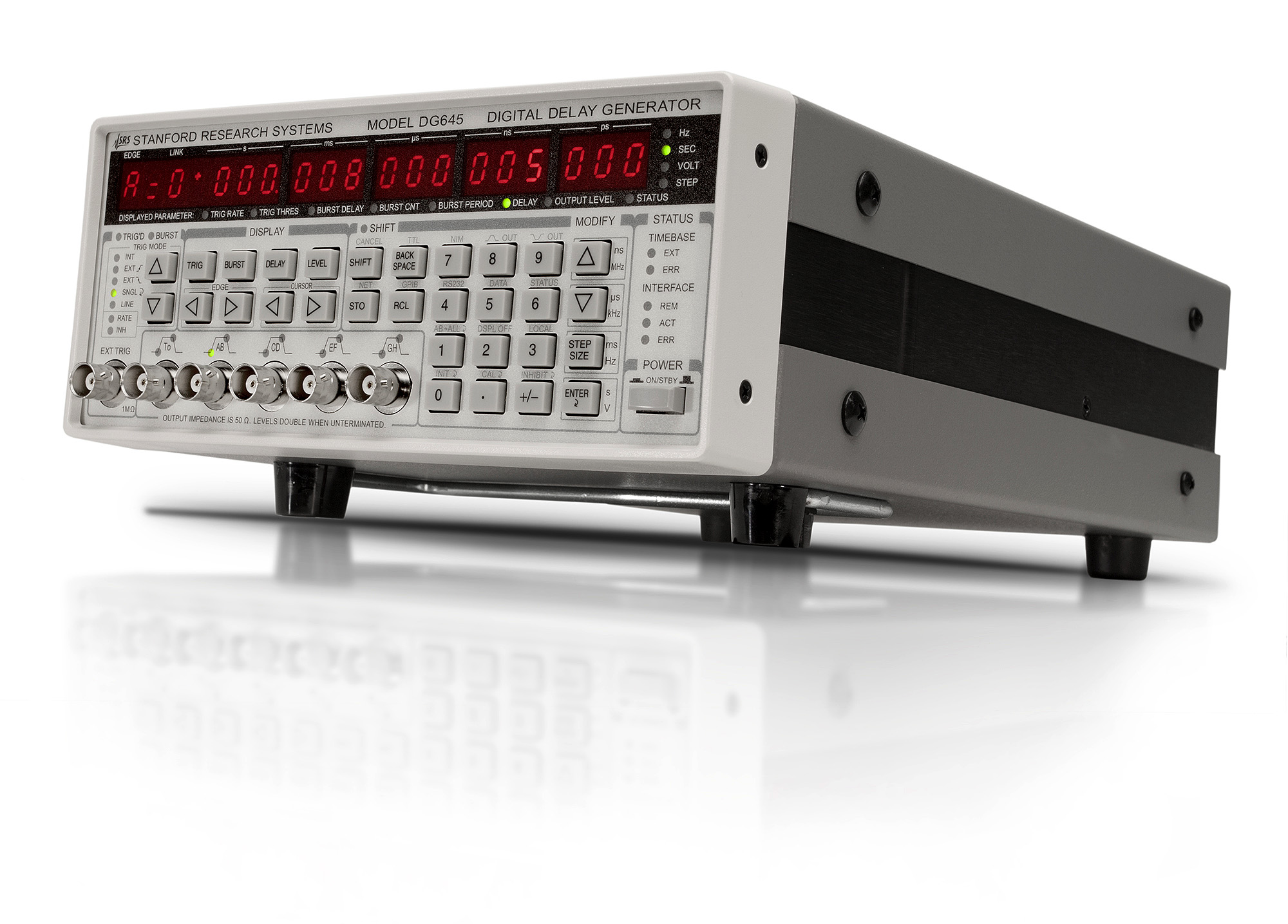
DG645
The DG645 is a versatile digital delay/pulse generator that provides precisely defined pulses at repetition rates up to 10 MHz. The instrument offers several improvements over older
Delay Generator Timing
All digital delay generators measure time intervals by counting cycles of a fast clock (typically 100 MHz). Most digital delay generators also have short programmable analog delays to achieve time intervals with finer resolution than the clock period. Unfortunately, one clock cycle of timing indeterminacy (typically 10 ns) can occur if the trigger is not in phase with the clock.
The DG645 eliminates timing indeterminacy by measuring the timing of triggers with respect to the internal clock and compensating the analog delays. This approach reduces the jitter by about 100× and allows the internal rate generator to operate at any rate—not just a sub-multiple of the clock frequency.
Triggering
The DG645 has many trigger modes. An internal rate generator, with less than 100 ps period jitter, may be set from 100 µHz to 10 MHz with 1 µHz resolution. An external trigger input, with adjustable threshold and slope, can trigger a timing cycle, a burst of cycles, or a single shot. A single shot can be triggered with a key press. A line trigger operates synchronously with the AC mains.
The DG645 supports a number of complex triggering requirements via a trigger holdoff and prescaling feature.
Trigger holdoff sets the minimum time between successive triggers. This is useful if a trigger event in your application generates a significant noise transient that needs time to decay away before the next trigger is generated. Trigger holdoff can also be used to trigger the DG645 at a sub-multiple of the input trigger rate.
Trigger prescaling enables the DG645 to be triggered synchronously with a much faster source, but at a sub-multiple of the original trigger frequency. For example, the DG645 can be triggered at 1 kHz, but synchronously with a mode locked laser running at 80 MHz, by prescaling the trigger input by 80,000. Furthermore, the DG645 also contains a separate prescaler for each front-panel output, enabling each output to operate at a sub-multiple of the trigger rate.
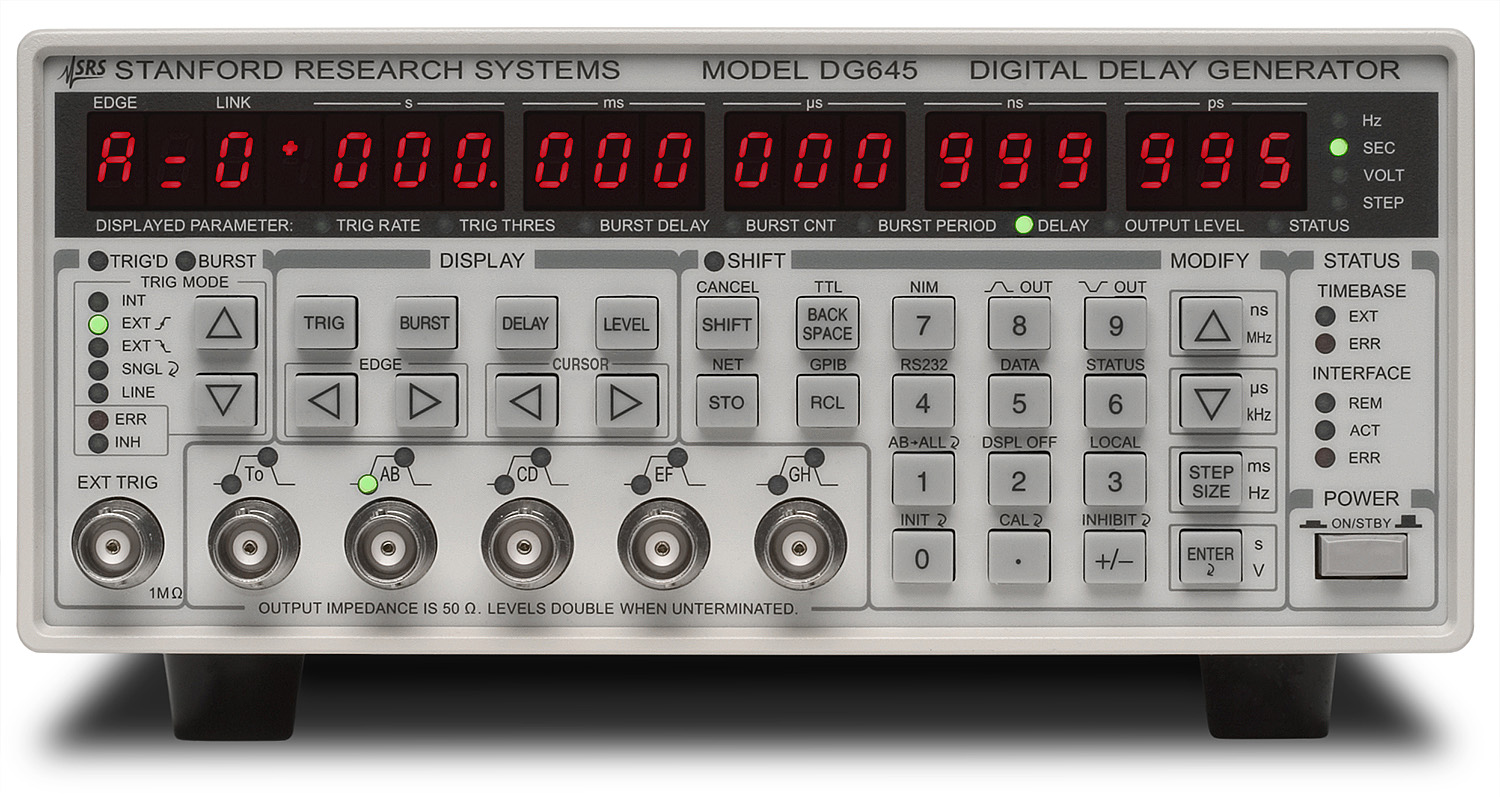
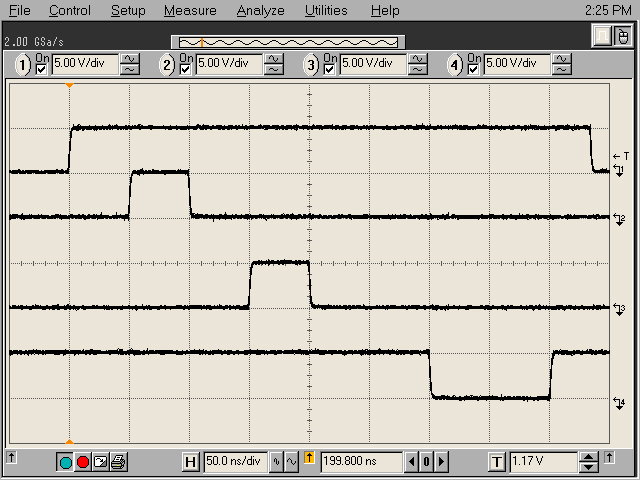
Front-Panel Outputs
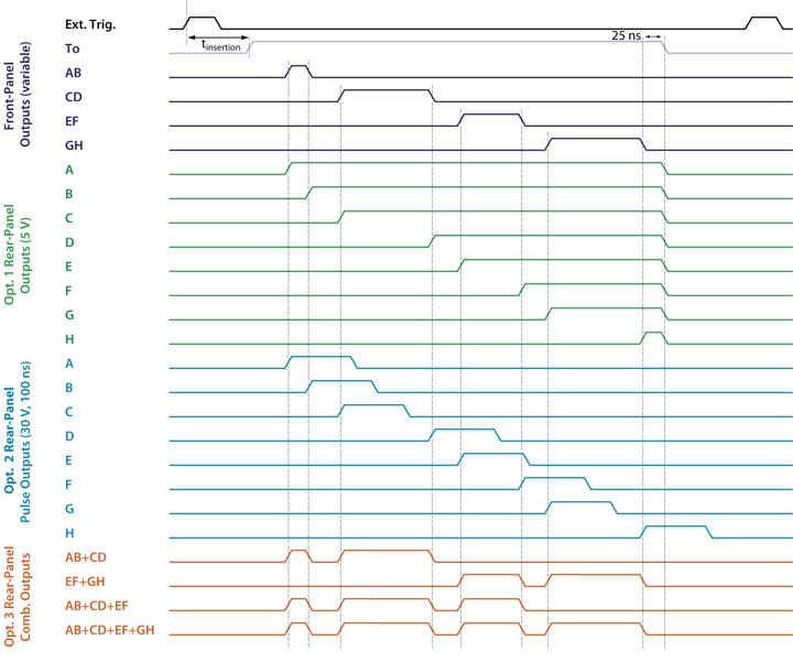
There are five front-panel outputs: T0, AB, CD, EF and GH. The T0 output is asserted for the duration of the timing cycle. The leading edge of T0 is the zero time reference. The programmed delays (A, B, C, D, E, F, G and H) are set from 0 s to 2000 s, with 5 ps resolution, to control the timing of the leading and trailing edges of the four pulse outputs.
Each front-panel output can drive a 50 Ω load and has a 50 Ω source impedance. Output amplitudes can be set from 0.5 to 5.0 V, and output offsets can range over ±2 VDC to source virtually any logic level (NIM, ECL, PECL, CMOS, etc.). Output transition times are less than 2 ns at any output amplitude.
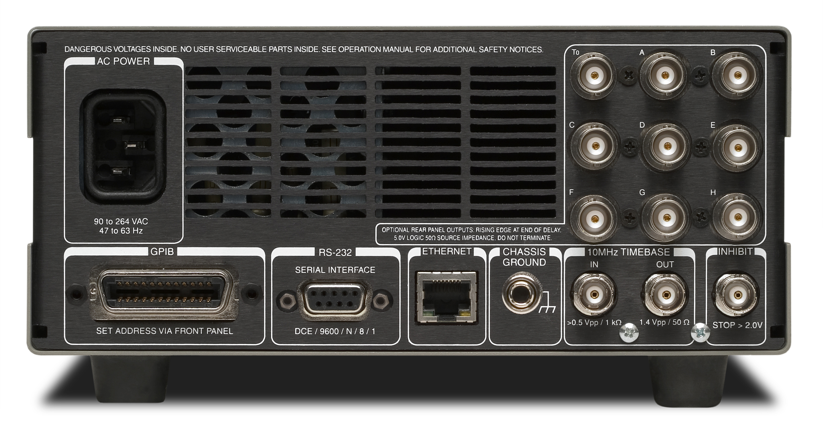
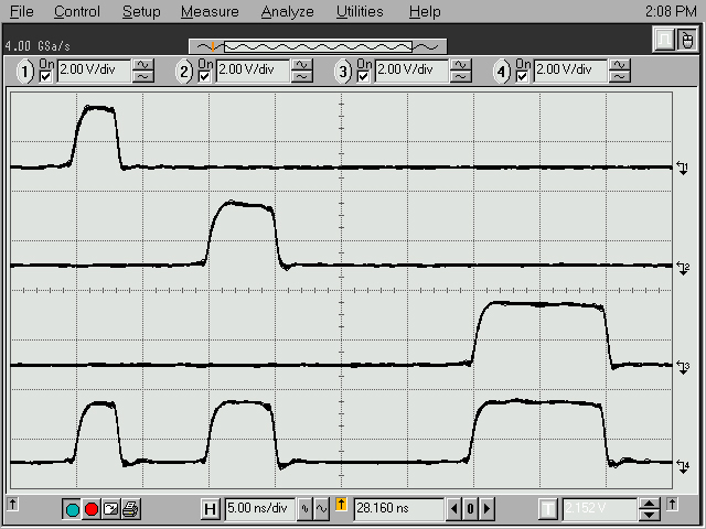
Rear-Panel Outputs
Optional rear-panel outputs are available to support diverse applications. Option 1 provides a T0 output and eight programmed delays (A, B, C, D, E, F, G and H) at 5 V logic levels, with transition times less than 1 ns. Option 2 provides these same outputs but as 30 V, 100 ns pulses with less than 5 ns transition times for timing distribution in high noise environments. Option 3 provides eight combinatorial outputs which deliver one to four pulses at 5 V logic levels with less than 1 ns transition times. Each output has a 50 Ω source impedance.
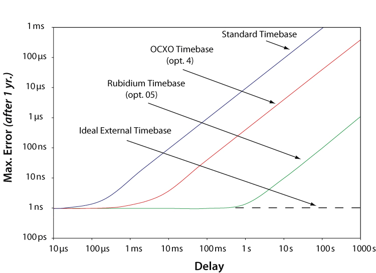
Timebases
The standard time base has an accuracy of 5 ppm, and a jitter of
The timing error for a 1 s delay can be as large as 5 µs for the standard timebase, 200 ns for the OCXO timebase, but is only 500 ps for the rubidium timebase (all one year after calibration.)
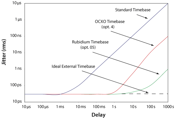
For short delays the jitter is typically 20 ps. However, for a 1 s delay, the standard timebase can contribute up to 10 ns of jitter, while the optional timebases contribute less than 10 ps of additional jitter.
Fast Rise Time Module
The DG645 front-panel outputs have transition times of less than 2 ns. The SRD1 is an accessory, built into an in-line BNC connector, which reduces the rise time of a front-panel output to less than 100 ps. Up to five SRD1s can be attached to the front panel to reduce the rise time of all of the outputs.